Creating a HomeKit Accessory
Overview
Over the past 8 weeks, I built a HomeKit accessory to open and close the gate at the end of my driveway. The project was really fun, and this document outlines the process of creating it, from concept to working prototype.
Additional Background
Programming examples for microcontrollers will be in C++. For the most part, we’ll be sticking essentially to “C with Classes”, which is typical of most Arduino and other microcontroller projects.
The data in this document is by no means meant to be comprehensive. I am not an electrical engineer, and welcome any corrections or other feedback. Where possible, I’ve cited references or resources I found useful at each step. For the most part, extensive googling served as the primary research tool.
The swing gate in question is a Sentex Crown Jewel, which was available in the early 2000s. It interfaces with a home phone system to control 1 or 2 relays. Programming is performed either via the gate keypad, or via 300 baud modem connected to a Windows program. Later in this document we’ll show how to use a listening modem to eavesdrop on the communication to reverse engineer the app-only commands which are not in the publicly available references.
Further data for those interested can be found
Concept
The problem I aimed to solve was to interface the gate microcontroller to HomeKit. The only interfaces to the gate are a keypad (outside the gate) and a home phone line. The previous owners did not install the manual operation switch, so I would frequently forget to open the gate when walking into town, get to the gate, then go back inside to dial the phone access code. It would be great to just pull out a phone or say “hey Siri open the gate”.
First thing to do is to decompose the goal into tasks small enough that each can have easily understandable requirements and success criteria. Another benefit of this process is that having many small tasks to complete will give us a sense of accomplishment and provide motivation as we complete them 🙂
Problem 1 - Phone Interface to Swing Gate
Objective: Implement software library that can send and receive phone number tones, and communicate with a 300 baud modem.
Success Criteria:
- Detect when phone is off hook, and listen for DTMF tones to keep HomeKit state in sync when other users control the gate from the phone line.
- Take phone off hook and dial numbers to control gate relay.
- Communicate via 300 baud modem (Bell 103) protocol.
Problem 2 - HomeKit Support
Objective: The microcontroller + phone line interface should appear as a home kit accessory.
Success Criteria:
- Successfully pair the device with HomeKit
- Implement a service that allows opening and closing the gate
- Demonstrate control via “Hey Siri open the gate”
Problem 3 - Physical prototype
Objective: Combine the proofs of concept of the phone interface, and homekit device, into a single logic board, have that board manufactured, and enclose it in a case.
Success Criteria:
- Capture a schematic which contains all necessary circuits for correct operation of the system.
- Arrange the physical design of those components and signals into a printed circuit board using a CAD program.
- Manufacture the board.
- Enclose the assembled board in a case so we can handle it safely and easily.
Phone Interface to Swing Gate
The first piece of the project is the phone line interface. Reviewing the requirements from earlier, our first requirement is “Detect when phone is off hook, and listen for DTMF tones”.
Decomposing this further, we need to:
- Understand how to interface a microcontroller to a phone line
- Understand how to take the phone “off hook”
- Do some signal processing to detect tones, for example, someone pressing the number “9” on a phone keypad.
Digital Access Arrangement
In the United States, home phone lines usually consist of a pair of wires, Tip and Ring, with a nominal -48VDC between them. These wires carry the signal (voice or data), and the voltage and resistance between them indicates various states (on hook, off hook, ringing, etc.) Additional info at Wikipedia.
Since the voltage on the lines (48v) is well above that typically interfaced to a microcontroller (1.8-5.0v), we need some circuitry to extract the signal from the phone line, convert it to a voltage compatible with our processor. Additionally, this circuitry should provide isolation of our circuitry from the phone circuit, to protect against transient voltage spikes. A nice discussion of isolation is here. In this application we’ve chosen to use a surge suppression capacitor that will fail open but magnetic isolation via a small transformer is also common in modem designs.
Since there are quite a few components in even simplified / cost reduced DAA’s (see page 21, <>) I opted to buy a reference board for the Ixys CPC5622 Litelink III DAA. Additional info can be found in the CPC5622-EVAL Evaluation Board Users Guide.
Integration With Arduino Uno
Connecting the Eval board for the Litelink DAA to the Arduino so that we can start looking at phone line signals is pretty straight forward. Looking at the Fritzing diagram below, we’ve connected an I2C oled to the Uno so we can see what’s happening. The eval board implements DC-blocking capacitors on the TX/RX lines, so we implement a voltage divider with a pair of resistors, and connect the RX line (pink) from the 5622 to A0 on the Uno, putting the “zero point” at 1.65V (3.3/2). We wire up a phone jack to the J1 header on the eval board, and we connect 3.3v through a 10k resistor to AREF on the Uno, setting the analog reference for ADC measurements at 3.3 * 32/(32+10) == 2.5v. Since the Uno doesn’t have a differential ADC, the Vpp (peak to peak voltage) on the RX+ line from the eval board should be <1V so we shouldn’t clip under normal operation, and get more precision out of the ADC by using more of its range vs. the standard 0-5V. “Off Hook” (orange) is pulled up as required by the 5622.
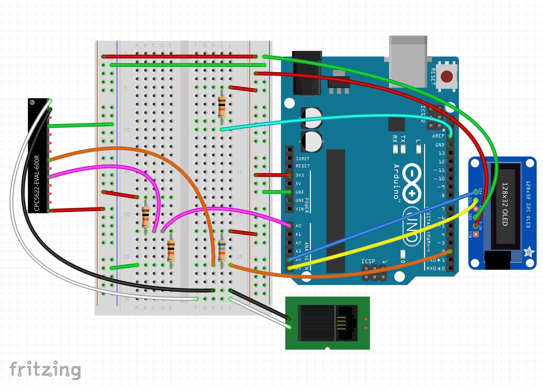
Success! At this point, we can read A0, and see the voltage held roughly constant at 1.65v when on hook, and if you pick up a receiver on the phone line connected to the 5622, you will start seeing the voltage vary as the call progress (dial) tone is received, or connect an oscilloscope and visualize it.
Digital Signal Processing
Now we have an analog signal into our Uno, and can move on to the next requirement: decode DTMF tones. Dual-tone multi-frequency (DTMF) is way each key on a phone key pad is converted into analog signals. The wikipedia article does a really good job summarizing what’s going on.
At this point we need to do some Digital Signal Processing (DSP) to figure out which frequencies are present in the signal we’re receiving, and then see if there are exactly two strong signals that happen to be one of the 16 DTMF pairs.
I’m not going to go too deeply into DSP here, but for a better understanding of what we’re trying to do, I cannot recommend these two resources highly enough.
-
Intro to DSP: This website has amazing interactive tutorials that explains some of the fundamentals of digital signal processing in a really neat and useful way.
-
DSP book: This book is a wealth of information on DSP techniques, and the PDFs of each chapter are available for free. With some effort, you can even concatenate them together into the entire book :)
Tone Detection
For DTMF, the typical sequence we are looking for is >=100ms of tone and >=100ms of silence repeated for however many digits we are listening for.
The common approach to frequency detection is an FFT. However, the performance of the 16MHz ATMega328P makes this difficult. For example, we need the FFT bins about 70Hz apart or less to discriminate the DTMF tones. So that means at 8KHz we need roughly 8000/70 = 114 samples or more. Rounding up to a convenient power of 2 for the FFT, we’ll say 256/2 = 128 FFT bins. The bins will be 8KHz / 128 = 62.5Hz apart.
To do a 256 sample FFT, in addition to a reasonable amount of memory, we’d need something on the order of ~8k multiplies and ~8k additions, which given the performance of 16x16+32 MAC is around 50 cycles, our most wildly optimistic projection here if we hand coded a great FFT is like 25-30ms, or about 0.5x realtime. This seems to line up well with the results on this Arduino FFT post. We also use the same performance hack noted there to reduce the ADC prescaler on the ATMega328 so that ADC reads don’t take so long.
An alternative approach is to use Goertzel algorithm which is essentially a single-frequency digital filter. Doing 8 applications of the Goertzel algorithm including the ADC reads only takes about 12ms, which is about 1.2x realtime. I think, based on the output of https://godbolt.org that AVR GCC is generating full 32x32 multiplies for 16x16+32 -> 32 MAC so some hand assembly could probably make this go faster.
In order to generate some test cases for our code, I used this DTMF WAV file generator and converted the resulting WAV files into virtual ADC samples in the range of our analog circuit. I then ran our detection code, to verify the algorithm correctness before moving it to the Uno. A reasonable sample Goertzel implementation can be found here
Bell 103
Programming the gate microcontroller is done via the 300 baud modem protocol Bell 103. The RX side of this seems well within the Uno’s capabilities, as we can likely count the number of zero crossings in every 3ms baud window to discriminate between the mark and space frequencies used by the FSK encoding.
The TX side however, seems much trickier on the Uno. The Uno lacks a DAC, and while you can create one using PWM on a digital pin and then put it through a low pass filter, this seemed like a lot of work. About this time I also wanted to get going on HomeKit portion of the project, and I took the easy way out: using an actual modem.
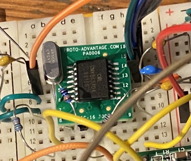
CMX865A Modem
Browsing Mouser & Digikey for modem ICs, I came across the CMX865A which is a single chip modem that costs a couple bucks, and is capable of detecting and generating DTMF and call progress tones, and talk the various 300/1200/2400 baud modem protocols.
The CMX865 is driven via C-Bus which is compatible with SPI. The IRQ line is connected to a microcontroller GPIO so that the modem can let us know when it has data or has detected a particular tone. The application nodes include sample code in a pseudo-assembly format for common tasks, see “CMX865A: Addressing SIA Protocols with the CMX865A” on the Application Notes section of the product page, which requires registration to download.
For the purposes of prototyping, I mounted the SOIC on a DIP adapter and mostly followed Figure 4 & 5 in the datasheet.
Summary
At this point, we can meet all the requirements for solving Proble 1. The CMX865A will handle the DTMF and Bell 103 work, and the CPC5622 will be our DAA, and a CPC5712 (from the CPC5622 eval board) will let us know when the line is in use by another handset.
HomeKit Support
Not sure where to begin on HomeKit support, I looked at some tear downs of various HomeKit devices:
Rachio Gen3: Based on a Murata Type1GC Module, which in turn is programmed via Cypress WiCED. WiCED theoretically supports HomeKit, but only if you’re a MFi certified company.
Eufy Camera: Based on a HiSilicon Hi3518, this is an ARM926-based SoC. BGA soldering, likely a linux board given the CPU has an MMU. Too big of a jump from the Uno for me, even assuming I could find a vendor for the chips.
HomeBridge on a Raspberry Pi: This actually seems like a pretty credible option, but didn’t I didn’t really want to buy a Pi and then interface the modem to it in Linux, again, a bit too big of a step up from the Arduino Uno.
More googling resulted in finding the Espressif HomeKit SDK. Espressif has a non-commercial SDK available for people who aren’t MFi license holders, in two flavors, a direct port of the HomeKit ADK and their own HomeKit SDK, in MFi and non-MFi flavors. For this project I used this latter one.
Choosing a Microcontroller
Espressif has several chips to choose from. The ESP8266 has been a popular for adding WiFi to projects for cheap. The ESP32 comes in single and dual core, also integrates an ethernet MAC.
I chose the ESP32-S2, since it’s available in several low cost dev boards, and I didn’t need multiple CPU cores. The S2-Saola I used is available for about $8.
I’m excited to try the ESP32-C3 coming up which has a RISC-V, but it wasn’t out yet at the time I did this project.
Installing the SDK
The getting started guide was easy to follow, and worked on my macOS 10.15 system. Plugging the USB cable into the port on the Saola board, and using the idf.py script included with the esp-idf SDK, I was able to flash and monitor over serial some of the included examples.
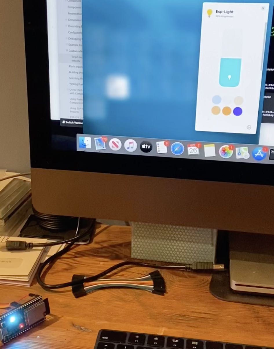
For instance, the Saola S1 includes a WS2812 RGB LED, sometimes referred to as the “neopixel”. The remote control interface example drives the RGB LED connected to GPIO18 on the dev board.
The typical set of steps is something like:
- ‘cd’ into sample project directory
- idf.py settarget esp32s2
- idf.py flash monitor
HomeKit Overview
For an in-depth overview of what HomeKit is and how it works, you can check out the main HomeKit website which has a link to the non-commercial protocol spec.
To summarize the basic design features of homekit:
- A homekit “accessory” is a device implementing one or more “services”
- A “service” is one of a couple dozen different types of things that homekit knows about (thermostat, air quality sensor, light switch, etc.)
- A “service” has a number of mandatory and optional “characteristics”. Current state. Target state. Color of a light. Parts per million of carbon dioxide, etc.
- An “accessory” has a primary type of service, but can implement any number of other services. So you can have a “Garage Door” that is also a light switch, and an air quality sensor.
- You can have a HomePod, AppleTV, or iPad to act as a home hub to manage interaction with the devices and run automation.
HomeKit devices communicate either over Bluetooth (which I have no experience with) or WiFi. The Espressif non-commercial SDK does not appear to have support for Bluetooth HomeKit devices. Nordic appears to, but like Cypress, their SDK is for MFi licensees only
Accessories are discovered by advertising an mDNS service. Not responding in a timely manner to mDNS queries will result in your device being marked unavailable in the Home app. Turning off WiFi power save and placing it in an area with good WiFi coverage seems to dramatically improve reliability.
HomeKit Demo - RGB Light
You can easily combine the RGB LED on the Saola board example and the homekit lightbulb example in the Espressif HomeKit SDK examples to create an RGB light bulb accessory that you can control through HomeKit.
HomeKit Gate Control
The final piece of solving our second problem is to pick an appropriate HomeKit accessory type, implementing it, and writing the necessary support code.
The “Garage Door” HomeKit accessory profile seemed to match with what we wanted. The only small gotcha is that the Garage Door accessory has a mandatory “obstruction detected” characteristic which we will just hardcode to false.
Building off the lightbulb example above, I created a FreeRTOS task (basically, a thread) that itself spins up two tasks, one to debounce the “Line In Use” GPIO. Line in use is used to know when to start listening to the phone line when someone else picks up the phone to open or close the gate. The second additional task actually runs the SPI interface to the modem to do the listening. The main task then blocks on a queue waiting for work from HomeKit to open/close the gate, and posts notifications back to the HomeKit task when the state changes.
Summary
We now have a fully working prototype, spread across several boards, of a HomeKit “garage door” which can open and close the gate by dialing the access code on the phone line, and can listen to other phones doing the same to keep state in sync. However, it’s spread across 3 separate boards, and has a habit of breaking when small children enter the office and knock it on the floor.
Physical Prototype
This was really the fun part of the project for me, and an area where there’s a huge and vibrant “community” on twitter and elsewhere. There are some seriously talented people out there making and documenting electronics. As above in the software section, I’ll link to most of hte resources that I found useful in making stuff work easily for me.
CAD Tools
We have two main tasks to carry out at this point in the project, where we are trying to make a single Printed Circuit Board (PCB) that contains all the necessary parts.
-
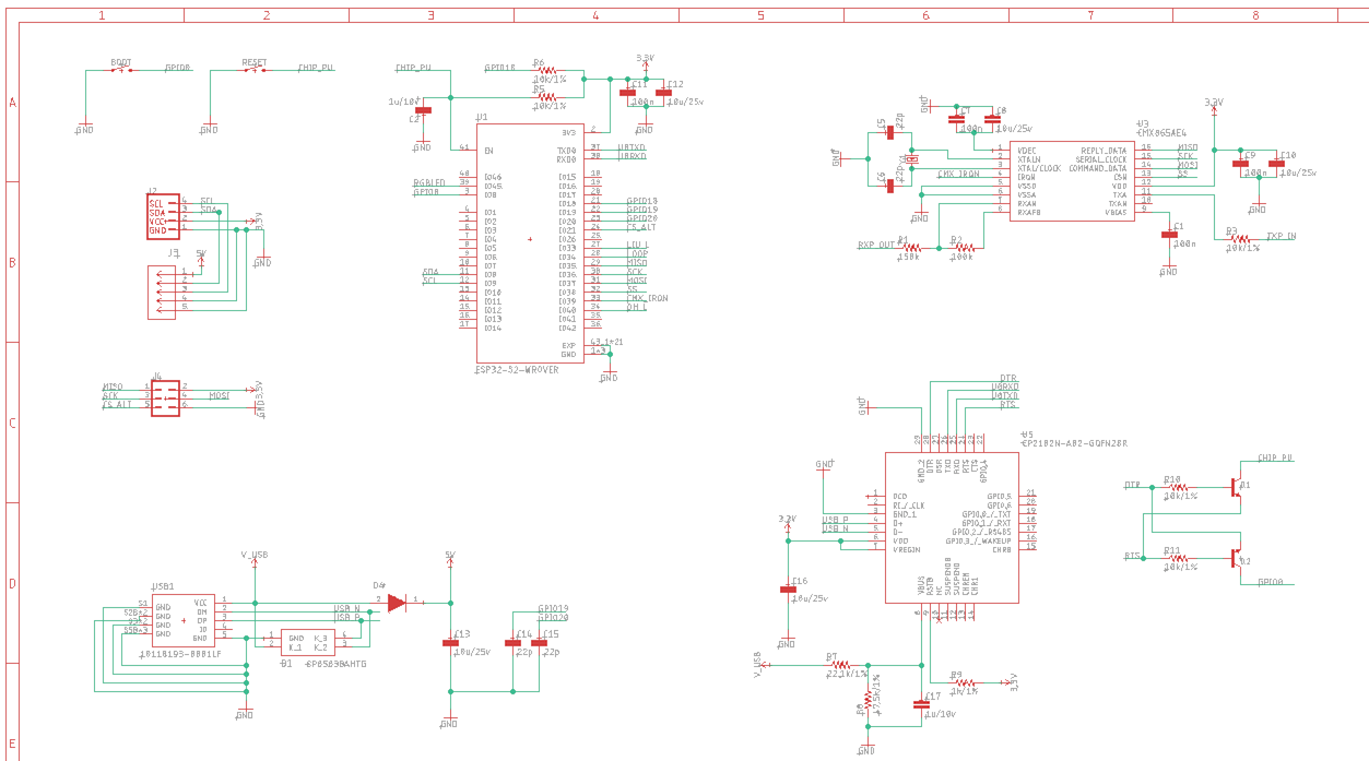
Schematic Capture - This is where we want to add all the parts to the project, and create diagrams of each subsystem, making sure all the right things are connected together.
-
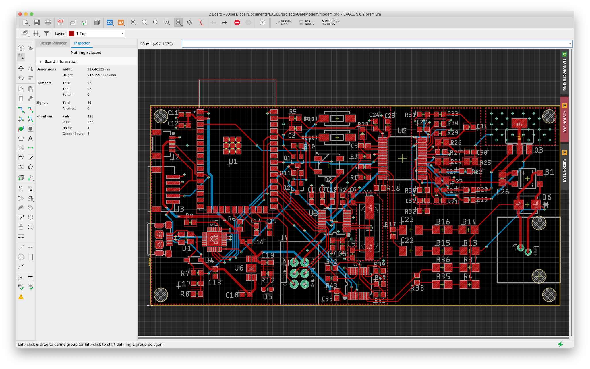
Board Layout - This is where we arrange the physical parts, and draw the copper wires and fills that will connect all the parts together.
From a previous Fusion360 project, I already had a copy of EAGLE, so that’s what I used for this project. It seems like most of the community these days is pretty interested in KiCAD, which looks great. I hope to use it on an upcoming project.
One of the nice things about the EDA space is that all the software does more or less the same thing. Everyone needs to capture schematics. Everyone needs to lay out boards. Everyone needs to import or create parts, etc. This means that youtube tutorials, even if they’re not for your specific EDA package, can be very helpful.
In particular I’d like to call out this video as being a comprehensive “so you want to make a microcontroller PCB” resource. It’s long, but it really does cover almost every aspect of the schematic capture and board layout.
SparkFun also has some great tutorials for EAGLE:
Schematic Capture
One of the first gotchas when starting out with EDA tools like EAGLE is that while they will have many parts in their “standard” library, they probably won’t have most of the specific ICs we’re looking for when creating the schematic.
For that, I’ve found it’s super useful to have accounts with the various databases of parts, such as:
These sites will let you search for a part number, such as the CPC5622 in our design, and download the schematic symbol, board layout footprint, and sometimes a 3D STEP model of the part to use.
Importing parts in EAGLE is not amazing, but it is pretty easy once you get the hang of it. There are essential two options:
- You download an EAGLE library (.lbr file), place it in ~/Documents/EAGLE/Libraries and then it is available for use.
- You open the library manager, open or create a library for your commonly used parts, and run a script (.scr file) which generates the symbol and footprint for you.
If you love pain and suffering, you can create your own symbols and footprints by reading design drawings from the manufacturers, and can follow the tutorials from SparkFun for creating custom parts in EAGLE.
Adding 3D Models to EAGLE Libraries
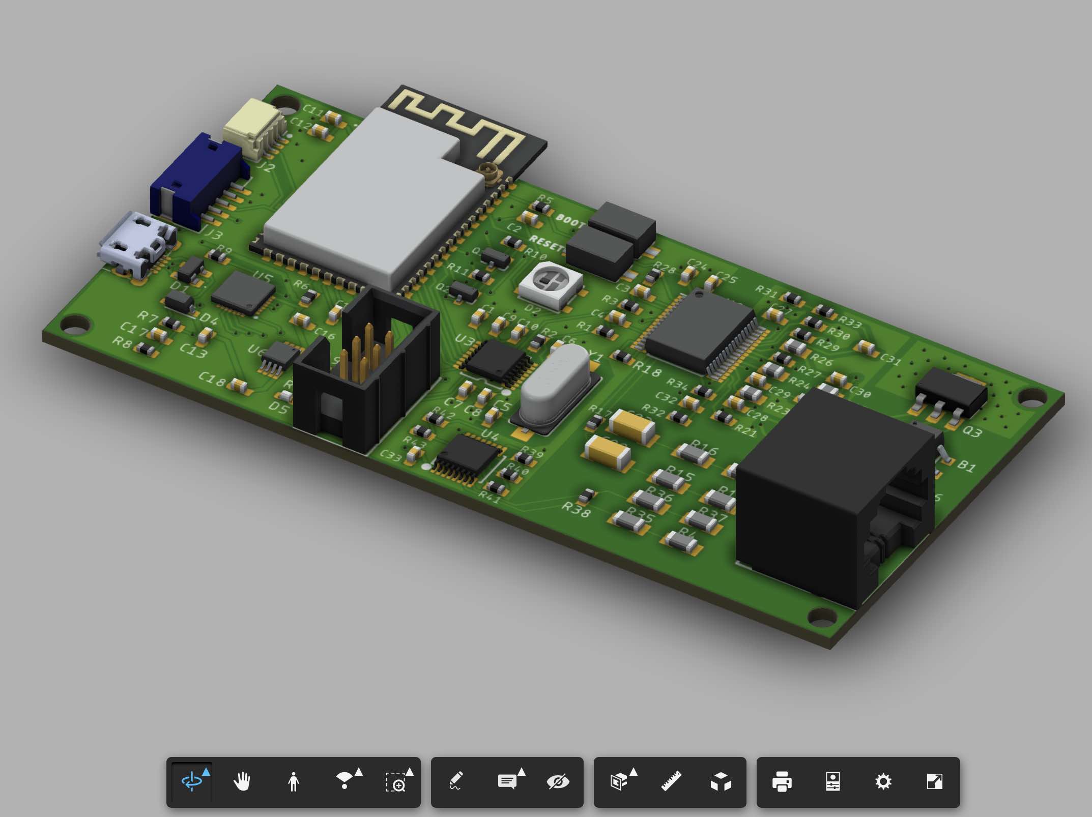
One of the most frustrating things that can happen is when you get your amazing PCB back from the factory, and you (or they) can’t solder a part to the board because you got the footprint wrong. It’s rare, but I have had parts with wrong footprints from the sites listed earlier, and I have made mistakes creating footprints from scratch by reading drawings. In all cases, these errors are easily caught by inspecting the 3D package in EAGLE which shows how the 3D part lines up with the pads on the board.
The other benefit is that you can make pretty pictures by pushing your model to Fusion360 where you can do all sorts of fun things to it, like Derive a Case or just spin it around
EAGLE has a few quirks around importing 3d models for parts, namely, they only really work well with Managed Libraries. A Managed Library in EAGLE is one that has been version controlled and uploaded to library.io. My library workflow is something like this:
When beginning to use EAGLE, create a new blank library, use the EAGLE command to convert it to a managed library, and save it. Then for each part you need:
- Download a .lbr from one of the part databases, and and then add the part from it to your library, OR run the .scr from one of the part databases to create the part in your library, OR create a new symbol/footprint/package yourself from scratch.
- Save the library, which will now say it has local modifications vs. the remote copy on library.io
- Use the menu command to “create new version”, which will generate a temporary 3D package as part of upload
- You can now open the 3D package editor for the library part, and either use the package generator to generate one for common IC shapes, or upload a STEP file (for connectors, LEDs, etc.)
- Save & create new version again.
It’s just that easy 😂
Board Editor
I am by no means a PCB routing expert, but I found these bits of advice from others to be generally useful.
- Try not to use the autorouter when you’re learning. It’s a fun puzzle to figure out where to place things to keep things tidy and correct. Like the CP2102N usb to serial chip having its pins backwards from the USB micro b connector.
- While your board manufacturer can probably handle things like 4 mil trace width and spacing, it may increase cost and there’s no particular need to be that aggressive in most designs, and it can allegedly lead to failure.
- Very small drill sizes can increase the cost of board manufacturing.
In terms of actually placing the components and routing them, I found the methods from the earlier Youtube video to result in working designs, with relatively little stress: First roughly position the various components together in functional groups. An IC and its crystal and decoupling caps, etc. Then move stuff together to fit in the board footprint you want First route the important things: power, crystal signals, etc. Finally move on to routing the rest of the signals.
For parts like the ESP32 which have GPIO muxes or other flexible I/O assignments, you can frequently save yourself a lot of trouble by picking pins on the package that make your routing job easy.
It is occasionally important to impedance match traces, such as for an antenna. Web calculator for trace impedance.
Saw several recommendations for Saturn PCB Toolkit, but sadly there is no mac version.
This is a simple calculator for determining the resistance of a trace, and the temperature rise with a given amperage flowing through it.
Once you have a finished PCB layout, the next step is to actually have it made. This process consists of two main steps:
- manufacturing the board
- assembling the components.
As my soldering skills are somewhere in the range of “bad, but functional”, I was looking for a company that would perform both jobs at reasonably low cost.
Choosing a manufacturer
There are lots of places that provide these services, with a wide range of cost, and varying capabilities. For hobbyists, it seems like there’s two main ones for assembly:
-
PCBWay: Boards, Stencils, Assembly, a lot of fun items in the gift shop.
-
JLPCB: You can see the ordering process for JLPCB as part of the earlier microcontroller schematic capture and pcb layout video.
I’ve seen dozens of good results from both of these manufacturers on twitter. Ultimately, the flexibility and great customer service at PCBWay lead me to use them for most of my projects.
If you’re interested in just having boards made (no assembly) and want them in purple, Oshpark https://oshpark.com also seems to have a lot of positive reviews and is in the US.
Uploading Design
In order to have our design manufactured, we need to have EAGLE generate a handful of files to upload to the manufacturer:
Gerber files, for which there will typically be one for every layer of the board. These are essentially commands to a computer to draw each “layer”, just as we had in EAGLE. Silkscreen, copper, solder mask, solder paste, etc. Drill file, which says which size drill bit to use and where to drill Pick n Place file, which says where the center of each part is, and how it is rotated A Bill of Materials (BOM) file, which we’ll cover in a bit.
In EAGLE, the CAM tool can easily generate all of these things. Just click the CAM tool in the board editor, which looks like a little factory. PCBWay requires CSV for the Pick N Place file, so select that in the CAM dialog for Assembly, and select CSV for Bill of Materials as well to allow easy import into a spreadsheet program as we’ll see below. Then check the export as zip file, mash “Process Job”. this is the Zip file we’re going to upload to PCBWay.
Making a BOM
The Bill of Materials (BOM) is essentially the list of parts needed to assemble the design. PCBWay provides a sample and a bunch of information and FAQs on their website here
EAGLE can export the BOM as a CSV, which is then easy to import into Excel / Numbers and match up the columns to the sample PCBWay BOM. The main thing you’ll typically be missing is manufacturer part numbers for passives like resistors or capacitors, and sometimes, full part numbers for ICs or connectors depending on how you’ve got your parts library set up.
What comes next can be a bit time consuming, perhaps there is a better way, but i’ve had good results by keeping some major parts distributors open, such as:
And then searching for the part e.g. “0603 100kOhm” and then seeing what seems to be commonly stocked that meets the specific needs (accuracy, temperature handling, etc.)
Once you’re done filling out the BOM, you can upload the BOM xslx, the Pick-n-Place csv from EAGLE, and the Gerbers and Drill file produced by the CAM job. An engineer reviews the design for manufacturability, and a quote for however many copies of the BOM are required to assemble the number of boards you’ve ordered is sent to you for approval.
If you approve the cost, PCBWay assembly takes a couple weeks, and then you get shiny new boards in the mail.
Process for JLPCB covered here.
For PCBWay, here.
Creating an Enclosure
I found this tutorial to be a pretty nice look at how to derive a simple case for a PCB, using EAGLE and Fusion360.
I followed a similar process and was largely successful, however, I still haven’t quite mastered 3D printing snap fit cases that work reliably. Watching videos like this where their case just snaps together with almost no visible seam is something I have yet to pull off successfully.
A good overview of fastening 3d printed parts. I had good results printing screw threads for M3 or larger, and using a tap cutting tool for M2. leaving a slot to capture a square or hex nut is probably also a good approach.
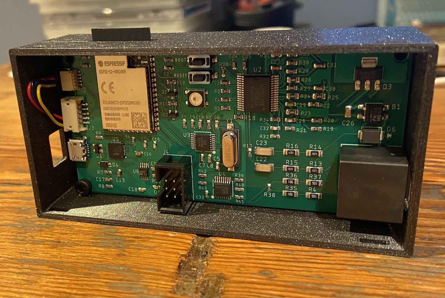
Here’s a video and photo of what we ended up with: